| Pressure | Resistance |
| No force | 0 Ω |
| Light force | .5 kΩ |
| Forceful | 2.0 Ω |
| Max force | 1.1 Ω |
2. 7 Segment display:
a. Check the manual of 7 segment display. Pdf document’s page 5 (or in the document page 4) circuit B is the one we have. Connect pin 3 or pin 14 to 5 V. Connect a 330 Ω resistor to pin 1. Other end of the resistor goes to ground. Which line lit up? Using package dimensions and function for B (page 4 in pdf), explain the operation of the 7 segment display by lighting up different segments. (EXPLAIN with VIDEO).


a. By connecting inputs either 0 V or 5 V, check the output voltages of the driver. Explain how the inputs and outputs are related. Provide two different input combinations. (EXPLAIN with PHOTOs and TRUTH TABLE)
Video 2: Shows the different outputs from the display driver
 Figure 5: Shows the setup for the 555 timer
 Figure 6: Shows the output to the oscilloscope

Theoretical:
frequency: 1.44/((150,000+2*300,000)*1 e-6 = 1.92
duty cycle: 300,000/(150,000+2*300,000) = 0.4
Measured:
frequency: 1.4 Hz
duty cycle: 0.6
Video 3: Shows the 555 timer with the force sensing resistor.
Video 5: Shows how the XOR gate works.

Video 8: Shows the whole circuit
a. Check the manual of 7 segment display. Pdf document’s page 5 (or in the document page 4) circuit B is the one we have. Connect pin 3 or pin 14 to 5 V. Connect a 330 Ω resistor to pin 1. Other end of the resistor goes to ground. Which line lit up? Using package dimensions and function for B (page 4 in pdf), explain the operation of the 7 segment display by lighting up different segments. (EXPLAIN with VIDEO).
Video 1: Shows how the 7 segment display works while moving a resistor.
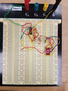
b. Using resistors for each segment, make the display show 0 and 5. (EXPLAIN with PHOTOs)
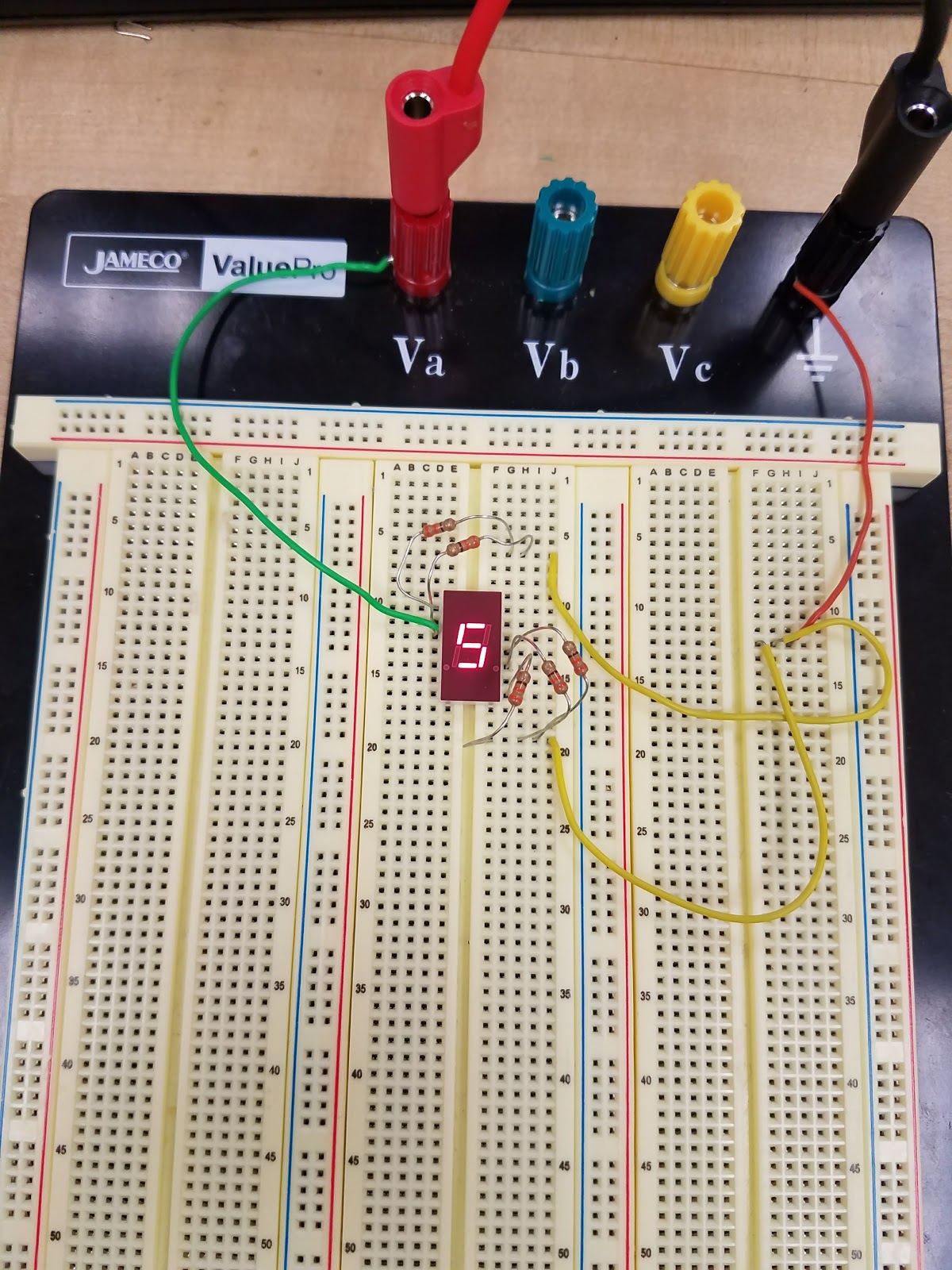
Figure 1: Shows 5 on the 7 segment display

Figure 2: Shows 0 on the 7 segment display
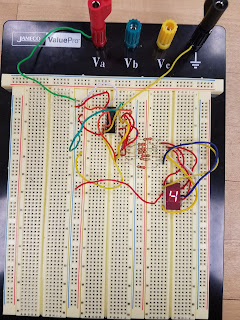
3. Display driver (7447). This integrated circuit (IC) is designed to drive 7 segment display through resistors. Check the data sheet. A, B, C, and D are binary inputs. Pins 9 through 15 are outputs that go to the display. Pin 8 is ground and pin 16 is 5 V.a. By connecting inputs either 0 V or 5 V, check the output voltages of the driver. Explain how the inputs and outputs are related. Provide two different input combinations. (EXPLAIN with PHOTOs and TRUTH TABLE)

Figure 3: Shows 0 using the display driver

Figure 4: Shows 4 on the display driver
| Display: | D | C | B | A |
| 0 | 0 | 0 | 0 | 0 |
| 4 | 0 | 1 | 0 | 0 |
b. Connect the display driver to the 7 segment display. 330 Ω resistors need to be used between the display driver outputs and the display (a total of 7 resistors). Verify your question 3a outputs with those input combinations. (EXPLAIN with VIDEO)
4. 555 Timer:
a. Construct the circuit in Fig. 14 of the 555 timer data sheet. VCC = 5V. No RL (no connection to pin 3). RA = 150 kΩ, RB = 300 kΩ, and C = 1 µF (smaller sized capacitor). 0.01 µF capacitor is somewhat larger in size. Observe your output voltage at pin 3 by oscilloscope. (Breadboard and Oscilloscope PHOTOs)


b. Does your frequency and duty cycle match with the theoretical value? Explain your work.

Theoretical:
frequency: 1.44/((150,000+2*300,000)*1 e-6 = 1.92
duty cycle: 300,000/(150,000+2*300,000) = 0.4
Measured:
frequency: 1.4 Hz
duty cycle: 0.6
c. Connect the force sensing resistor in series with RA. How can you make the circuit give an output? Can the frequency of the output be modified with the force sensing resistor? (Explain with VIDEO)
5. Binary coded decimal (BCD) counter (74192). This circuit generates a 4-bit counter. With every clock change, output increases; 0000, 0001, 0010, …, 0111, 1000, 1001. But after 1001 (which is decimal 9), it goes back to 0000. That way, in decimal, it counts from 0 to 9. Outputs of 74192 are labelled as QA (Least significant bit), QB, QC, and QD (Most significant bit) in the data sheet (decimal counter, 74192). Use the following connections:
5 V: pins 4, 11, 16.
0 V (ground): pins 8, 14.
10 µF capacitor between 5 V and ground.
a. Connect your 555 timer output to pin 5 of 74192. Observe the input and each output on the oscilloscope. (EXPLAIN with VIDEO and TRUTH TABLE)
| Counter | Qd | Qc | Qb | Qa |
| 0 | 0 | 0 | 0 | 0 |
| 1 | 0 | 0 | 0 | 1 |
| 2 | 0 | 0 | 1 | 0 |
| 3 | 0 | 0 | 1 | 1 |
| 4 | 0 | 1 | 0 | 0 |
| 5 | 0 | 1 | 0 | 1 |
| 6 | 0 | 1 | 1 | 0 |
| 7 | 0 | 1 | 1 | 1 |
| 8 | 1 | 0 | 0 | 0 |
Figure 7: Shows the Truth table for the 74192
Video 4: Shows the frequency changes with different outputs
6. 7486 (XOR gate). Pin diagram of the circuit is given in the logic gates pin diagram pdf file. Ground pin is 7. Pin 14 will be connected to 5 V. There are 4 XOR gates. Pins are numbered. Connect a 330 Ω resistor at the output of one of the XOR gates.
a. Put an LED in series to the resistor. Negative end of the LED (shorter wire) should be connected to the ground. By choosing different input combinations (DC 0V and DC 5 V), prove XOR operation through LED. (EXPLAIN with VIDEO)
b. Connect XOR’s inputs to the BCD counters C and D outputs. Explain your observation. (EXPLAIN with VIDEO)
Video 6: Shows what happens when the XOR is connected to the 74192
c. For 6b, draw the following signals together: 555 timer (clock), A, B, C, and D outputs of 74192, and the XOR output. (EXPLAIN with VIDEO)
Video 7: Shows the signal outputs
7. Connect the entire circuit: Force sensing resistor triggers the 555 timer. 555 timer’s output is used as clock for the counter. Counter is then connected to the driver (Counter’s A, B, C, D to driver’s A, B, C, D). Driver is connected to the display through resistors. XOR gate is connected to the counter’s C and D inputs as well and an LED with a resistor is connected to the XOR output. Draw the circuit schematic. (VIDEO and PHOTO)

Video 8: Shows the whole circuit
We got different values for the pressure resistor. I am curious if they come in different values, because the extent of the difference is huge.
ReplyDeleteYou're binary table is wrong by the way. you forgot a value for 0.
0000 is 0
0001 is 1
0010 is 2
0010 is 3...
1100 is 9.
I would fix that table before Monday!
Yes you are right thanks Alec!
DeleteNice job this week, once you add number 8 and correct the truth table you should be good. Did you guys face any difficulties this week? we struggled a lot with the 555 timer for some reason and then for number 7 when implementing everything together. the issue ended up being a missing cable giving voltage to the 7447 driver. Our values for this week look quite similar except for the binary table. Nice job
ReplyDeleteYes we struggled a little bit with implementing the entire circuit together as well simply because of trying to figure out how to space everything out on the breadboard we didnt want everything to be right on top of each other so in case we made a mistake it would be easier to trouble shoot. Thanks for the input Joe.
Deletei think for q # 1 it will be better if you give more explanation why we are getting a low resistance value when we applied a high force in the FSR and why we are using it in the circuit.
ReplyDeleteYes, we believe our data may be slightly misleading and we probably should have included more values to make the trend of the FSR more apparent.
DeleteGood organization and explaination for most questions. I think you need to explain Q2 and 4 photos. Also, try to use full truths tables.
ReplyDeleteGood job.
Overall, I think you guys did a great job on your blog. You got most of everything to work and video 6 - the whole circuit - looked great. The oscilloscope looks good too, the first problem we had was our zoom was way to far in so we couldn't see it. But, everything looks good. Maybe use a bigger binary table though.
DeleteThanks guys we made those adjustments you suggested
DeleteWell Done. It might be a good idea to add more measurement values for number 1. Perhaps make some of the images larger, as they were hard to see.
ReplyDeleteThanks Nicholas yes I agree ideally we could have added more values so the trend is easier to see and we will be sure to make them larger for the future.
DeleteI like the way you set up your resistors in the first picture. For us we decided to set them right next to each other and that created a problem whenever they were touching. So we always had to be careful of that in our lab so we wouldn't get the wrong number or the circuit itself just wouldn't work. Also nice video's they get to the point.
ReplyDeleteThanks Mary! yes we tried to spread everything out as much as possible both vertically and horizontally to prevent shorts and make it easier to trouble shoot and adjust because there were so many components.
DeleteGood job, as usual guys! My only suggestion would be to do a complete truth table for 3a. What you have is correct so I am sure you both understand what the rest of it would look like, but other people reading your blog might find it useful.
ReplyDeleteLooks good.
ReplyDelete