| Pressure | Resistance |
| No force | 0 Ω |
| Light force | .5 kΩ |
| Forceful | 2.0 Ω |
| Max force | 1.1 Ω |
2. 7 Segment display:
a. Check the manual of 7 segment display. Pdf document’s page 5 (or in the document page 4) circuit B is the one we have. Connect pin 3 or pin 14 to 5 V. Connect a 330 Ω resistor to pin 1. Other end of the resistor goes to ground. Which line lit up? Using package dimensions and function for B (page 4 in pdf), explain the operation of the 7 segment display by lighting up different segments. (EXPLAIN with VIDEO).


a. By connecting inputs either 0 V or 5 V, check the output voltages of the driver. Explain how the inputs and outputs are related. Provide two different input combinations. (EXPLAIN with PHOTOs and TRUTH TABLE)
Video 2: Shows the different outputs from the display driver
 Figure 5: Shows the setup for the 555 timer
 Figure 6: Shows the output to the oscilloscope

Theoretical:
frequency: 1.44/((150,000+2*300,000)*1 e-6 = 1.92
duty cycle: 300,000/(150,000+2*300,000) = 0.4
Measured:
frequency: 1.4 Hz
duty cycle: 0.6
Video 3: Shows the 555 timer with the force sensing resistor.
Video 5: Shows how the XOR gate works.

Video 8: Shows the whole circuit
a. Check the manual of 7 segment display. Pdf document’s page 5 (or in the document page 4) circuit B is the one we have. Connect pin 3 or pin 14 to 5 V. Connect a 330 Ω resistor to pin 1. Other end of the resistor goes to ground. Which line lit up? Using package dimensions and function for B (page 4 in pdf), explain the operation of the 7 segment display by lighting up different segments. (EXPLAIN with VIDEO).
Video 1: Shows how the 7 segment display works while moving a resistor.
b. Using resistors for each segment, make the display show 0 and 5. (EXPLAIN with PHOTOs)
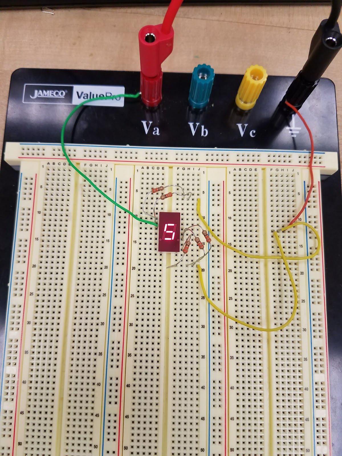
Figure 1: Shows 5 on the 7 segment display

Figure 2: Shows 0 on the 7 segment display
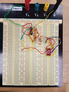
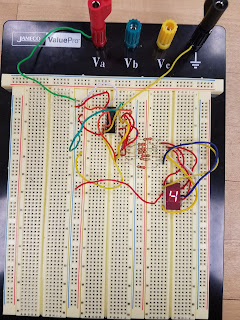
3. Display driver (7447). This integrated circuit (IC) is designed to drive 7 segment display through resistors. Check the data sheet. A, B, C, and D are binary inputs. Pins 9 through 15 are outputs that go to the display. Pin 8 is ground and pin 16 is 5 V.a. By connecting inputs either 0 V or 5 V, check the output voltages of the driver. Explain how the inputs and outputs are related. Provide two different input combinations. (EXPLAIN with PHOTOs and TRUTH TABLE)

Figure 3: Shows 0 using the display driver

Figure 4: Shows 4 on the display driver
| Display: | D | C | B | A |
| 0 | 0 | 0 | 0 | 0 |
| 4 | 0 | 1 | 0 | 0 |
b. Connect the display driver to the 7 segment display. 330 Ω resistors need to be used between the display driver outputs and the display (a total of 7 resistors). Verify your question 3a outputs with those input combinations. (EXPLAIN with VIDEO)
4. 555 Timer:
a. Construct the circuit in Fig. 14 of the 555 timer data sheet. VCC = 5V. No RL (no connection to pin 3). RA = 150 kΩ, RB = 300 kΩ, and C = 1 µF (smaller sized capacitor). 0.01 µF capacitor is somewhat larger in size. Observe your output voltage at pin 3 by oscilloscope. (Breadboard and Oscilloscope PHOTOs)


b. Does your frequency and duty cycle match with the theoretical value? Explain your work.

Theoretical:
frequency: 1.44/((150,000+2*300,000)*1 e-6 = 1.92
duty cycle: 300,000/(150,000+2*300,000) = 0.4
Measured:
frequency: 1.4 Hz
duty cycle: 0.6
c. Connect the force sensing resistor in series with RA. How can you make the circuit give an output? Can the frequency of the output be modified with the force sensing resistor? (Explain with VIDEO)
5. Binary coded decimal (BCD) counter (74192). This circuit generates a 4-bit counter. With every clock change, output increases; 0000, 0001, 0010, …, 0111, 1000, 1001. But after 1001 (which is decimal 9), it goes back to 0000. That way, in decimal, it counts from 0 to 9. Outputs of 74192 are labelled as QA (Least significant bit), QB, QC, and QD (Most significant bit) in the data sheet (decimal counter, 74192). Use the following connections:
5 V: pins 4, 11, 16.
0 V (ground): pins 8, 14.
10 µF capacitor between 5 V and ground.
a. Connect your 555 timer output to pin 5 of 74192. Observe the input and each output on the oscilloscope. (EXPLAIN with VIDEO and TRUTH TABLE)
| Counter | Qd | Qc | Qb | Qa |
| 0 | 0 | 0 | 0 | 0 |
| 1 | 0 | 0 | 0 | 1 |
| 2 | 0 | 0 | 1 | 0 |
| 3 | 0 | 0 | 1 | 1 |
| 4 | 0 | 1 | 0 | 0 |
| 5 | 0 | 1 | 0 | 1 |
| 6 | 0 | 1 | 1 | 0 |
| 7 | 0 | 1 | 1 | 1 |
| 8 | 1 | 0 | 0 | 0 |
Figure 7: Shows the Truth table for the 74192
Video 4: Shows the frequency changes with different outputs
6. 7486 (XOR gate). Pin diagram of the circuit is given in the logic gates pin diagram pdf file. Ground pin is 7. Pin 14 will be connected to 5 V. There are 4 XOR gates. Pins are numbered. Connect a 330 Ω resistor at the output of one of the XOR gates.
a. Put an LED in series to the resistor. Negative end of the LED (shorter wire) should be connected to the ground. By choosing different input combinations (DC 0V and DC 5 V), prove XOR operation through LED. (EXPLAIN with VIDEO)
b. Connect XOR’s inputs to the BCD counters C and D outputs. Explain your observation. (EXPLAIN with VIDEO)
Video 6: Shows what happens when the XOR is connected to the 74192
c. For 6b, draw the following signals together: 555 timer (clock), A, B, C, and D outputs of 74192, and the XOR output. (EXPLAIN with VIDEO)
Video 7: Shows the signal outputs
7. Connect the entire circuit: Force sensing resistor triggers the 555 timer. 555 timer’s output is used as clock for the counter. Counter is then connected to the driver (Counter’s A, B, C, D to driver’s A, B, C, D). Driver is connected to the display through resistors. XOR gate is connected to the counter’s C and D inputs as well and an LED with a resistor is connected to the XOR output. Draw the circuit schematic. (VIDEO and PHOTO)

Video 8: Shows the whole circuit


